产品中心
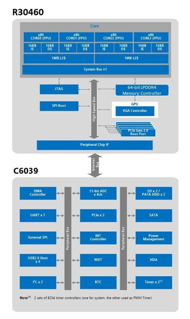
产品中心 R30460_C6039是一个32位处理器x86兼容平台系列。它包括一个32位四核处理器,R30460,包含LPDDR4控制器、内置图形核心、NB、SPI、PCIe Gen3.0和外围芯片C6039。C6039的主要功能包括SATA、HDA(高清音频)、SD卡、PCIe Gen1.1、I2C总线、UART、USB主机控制器和其他遗留接口。得益于功率优化的处理器架构,它为嵌入式和IPC市场提供了优势。这个操作系统兼容性包括DOS、WinCE、Linux、Windows XP、Windows Embedded XP、Windows 7、Windows 10和VxWorks操作系统。现在R30460_C6039平台支持AMI传统BIOS,并使用R8220 MCU进行平台的通电/断电序列控制。
产品应用
终端销售系统 公共信息机 人机界面应用 精简型计算机 | 嵌入式工业计算机应用 工业自动化控制设备 云端医疗系统 智能型自动贩卖机 | 自动提款机 车用信息娱乐系统 数字电子广告牌 |
R30460
● Quad RISC Processor Core@1.6GHz – Symmetric Multi-Processors – 6-stage pipeline – x86 instruction set P6 with SSE/SSE2/SSE3/SSSE3 ● Floating - Point Unit Support – Extends CPU instruction set to include Trigonometric, Logarithmic and Exponential – Implements ANSI/IEEE standard 754-1985 for binary Floating-Point Architecture ● Branch Prediction Unit – Branch target buffer ● Translation Lookaside Buffer – 4-Kbyte page I-TLB 64 entries/ 4-Kbyte page D-TLB 64 entries – 4-Mbyte page I-TLB 8 entries/ 4-Mbyte page D-TLB 8 entries ● Embedded I / D Separated L1 Cache – 4-way 16-Kbyte I-Cache, 4-way 16-Kbyte D-Cache – Write-through policy ● Embedded Unified Cache – 8-way 2MB L2 Cache – Write-through or write-back policy – LLC 4MB ● LPDDR4 Control Interface – 64-bit data bus, 3200Mbps – DRAM size maximum up to 16Gbyte | ● GPU Control Unit – VGA Controller – 2D Graphics Engine support – Supports Single Display max resolution up to 1920x1440@60Hz – Supports Dual Display max resolution up to 1280X1024@60Hz – Supports Display Device with one D-sub Analog Interface – Supports Display Device with one 24-bit DVO Digital Interface to connect a third party LVDS/HDMI/AVI transmitter ● PCI Express 3.0 – 8 lane (One 4-lane root port & Four 1-lane root ports) ● SPI Interface – For boot up function from SPI flash – Supports flash size up to 128Mbits – Supports 4 IO mode JTAG Interface Supported ● Input Clock – 25 MHz ● Operating Voltage Range – Core Voltage: 0.9V± 5% – I/O Voltage: 1.1V ± 5%, 1.8V ± 5%, 3.3V ± 5% ● Operating Temperature – -0℃~70℃ Package Type – FCBGA 27x27 |
C6039
● IDE Controller – PATA 100 (HDD x 2) or SD x 2 at Primary Channel – SATA 1.5Gb/s (1 Port) at Secondary Channel ● PCIe Control Interface x 2 – Up to 2 sets of PCIe devices – Compatible with PCI Express v1.1 ● HDA Controller ● 11-Bit ADC x 8 Channels – Effective Number of Bit=10 bits ● DMA Controller ● Counter / Timers – 2 sets of 8254 timer controllers (one for system, the other one used as PWM Timer) – Output on the 2nd PWM Timer Controller ● Real Time Clock – Less than 2.5uA (3.0V) power consumption in Internal RTC Mode while chip is power-off ● FIFO UART Port x 7 (7 Sets of COMPort) – Compatible with 16C550 / 16C552 – Default internal pull-up – Supports the programmable baud rate generator with the data rate from 50 to 3Mbps – The character options are programmable for 1 start bit; 1, 1.5 or 2 stop bits; even, odd or no parity; 5~8 data bits – Supports TXD_EN Signal on COM1/2/3/4 ● I2C Bus x 2 – Compliant with V2.1 – Does not support master code of general call address, START and CBUS. | ● General-Purpose Programmable I/O – Supports 88 programmable I/O pins – Each GPIO pin can be individually configured as an input/output pin – GPIO_P0 and GPIO_P1 with interrupt support (input/output) ● USB 2.0 Host Support – Supports HS, FS and LS – 4 ports ● Speaker Out ● Input Clock – 14.318 MHz – 32.768 KHz ● Output Clock – 24 MHz – 25 MHz ● Operating Voltage Range – Vcore Voltage:1.2V ± 5% – I/O Voltage: 1.8V ± 5% , 3.3 V ± 10 % ● Operating Temperature – -25℃ ~ 85℃ ● Package Type – 19x19mm, 441-Ball LFBGA |